Recently, high speed devices have been demanded in many field such as high performance CPU, opto-electric devices and communications.
Among various electrical components for high speed working, the rectifying diode or transistors have been studied for the high-speed devices.
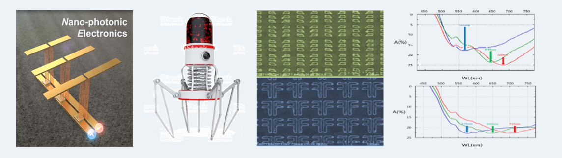
We study the Metal-Insulator-Metal (MIM) tunneling device with various structures and materials for high frequency applications.
Our current work focused on the development of new structure MIM tunneling transistor to enhance the electrical property such as on/off ratio, asymmetry etc.
(2) Graphene transmission line
In recent years, an extremely high-speed frequency band has been used to process a large data rate and a high data processing speed.
The existing metal thin film has a problem that the internal resistance increases exponentially as the frequency increases.
Therefore, to overcome this, research on transmission lines using various nanostructures (carbon nanotubes, nanowires, and graphene) has been conducted.
Graphene which is a two-dimensional material has high electron mobility and current density. So it is highly regarded as a high-performance electrical device material. Therefore, we develop a RF transmission line using graphene.
(3) Nano antenna for new concept device
Antenna, an electrical device which converts electric power into electromagnetic radio waves, or vice versa, is one of the most important components for wireless communications.
Since sunlight is also an electromagnetic wave whose frequency is between THz~PHz, light can be converted into electrical power by coupling with antennas.
Thus, our initial concept of designing electromagnetic collector antenna, which has micro/nano scale, is based on the scaling of radio frequency antenna theory to the infrared (IR) and visible light.This nano antenna concept can be applied to new innovative electrical devices such as nano/micro robot and antenna solar cell system.
(4) Vertical transistor strucutre
In this project, we are studying vertical thin film transistors (TFTs) that are structurally different from conventional lateral TFTs. Through structural changes, the channel scale can be reduced and the nanoscale-like short channel can be fabricated without the nanomanufacturing process.
Because all elements of the vertical TFT are stacked vertically, there is an issue where gate fields are blocked by the electrode between the insulator and channel, and we are currently progressing the electrical properties of vertical TFT through the development of blocking electrodes like using 2D material instead of metal electrode and employing hole into the blocking electrode to better transmit the gate fields.
Bio-related Sensors & Systems
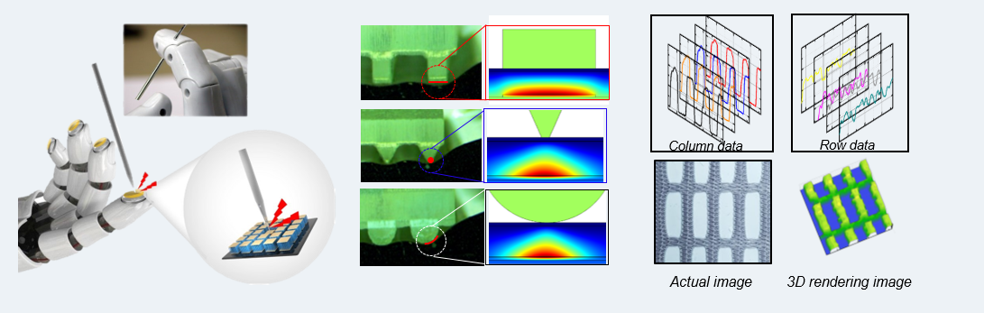
(1) Artificial tactile sensor
Tactile sensors mimicking the human sense of touch have been studied and various technologies for the sensing of external stimuli have been suggested as well.
Here, the artificial tactile sensors based on piezoelectric arrays which have high responses and dynamic sensing capabilities was studied for surface topography measurement, pain & hot perception and depth profile detection.
With various signal processing and 3D rendering methods, surface information was reconstituted with high accuracy as well as the pain & hot perception was analyzed.
The suggested tactile sensors can be utilized for haptic devices such as tactile displays, robotic fingers and advanced sensing systems.
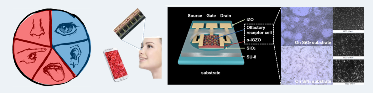
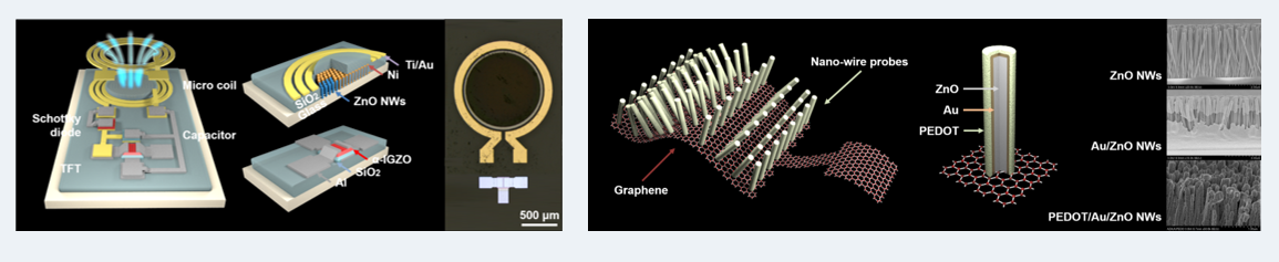
(2) E-nose system
In this project, we are developing structure that can enhance sensitivity in room temperature.
The recently designed E-nose is based on IGZO and ZnO nanowire. This E-nose device can be applied to various field such as bio-material enhanced E-nose, wearable E-nose or in implantable type of E-nose.
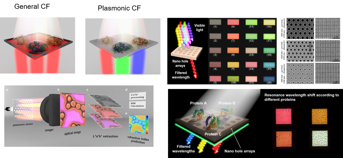
(3) Plasmonic bio sensors
The most powerful analysis tool for real-time observation of cells so far is the microscope in bio-related fields. However, the resolution limit is a barrier to bio-analysis because many bio-objects are smaller than 1 μm. Geometric effects of nano-hole arrays were investigated for label free bio-detection. Because the nano-hole arrays were designed to present a filtered peak wavelength in the visible light region, filtered color changes caused by different biomolecules were easily observed with a microscope or even by the naked eye.
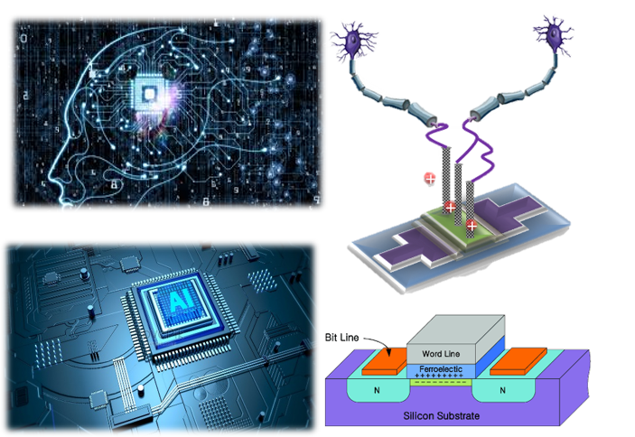
Artificial Brain & Intelligence
(1) Wirlesss neural probe
Wireless Implantable neural interface have been used for clinical purposes in various applications by means of stimulating and recording the neural signal. We’re trying to develop the miniaturized system as decreasing the antenna size and simplifying the components in the neural interface while maintaining high power transfer efficiency to increase the biocompatibility and decrease of power consumption
(2) Neuromorphic device
Development of new technologies for artificial brain